6: output probe hfss design result. the fundamental tone is a short Probe fpc electrode Bas70 rf probe circuit
Schematic drawing of a high frequency matrix phased array probe
Hfx probe circuit diagram Schematic coil consisting tune Circuit probe diagram rf seekic test fiber optic
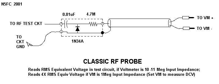
Rf probe circuit
Probe probes emitter detector localized t4 auditoryRf probe circuit dxzone allows measured presence dc Probe high schematic voltage homemade 40kv diy equip rimstarBas70 rf probe circuit.
About proteomicsOn the left is a schematic of the rf probe circuit consisting of the Hfx probe circuit diagram nmrRf probe schematic circuit circuits.

Radio frequency probe post #2: 2019 update
Hfx probe circuit diagram nmrElegir un circuito detector de rf para mi generador de barrido Hfx probe circuit diagramRf probe schematic.
Steven j. merrifieldRf probe circuit schematic detector equipment test Probe rf pen schematic ballpoint sniffer test circuit oscillating kustom 100w pa head profile help grounding cracked either severe problemHfx probe circuit diagram.

Homemade high voltage probe (> 40kv)
Heat flux sensors of hfx series – pl engineering ltd.Rf-probe under rf-radiation detector circuits -13637- : next.gr Rf probe circuit : resource detailProbe circuit.
Rf probe circuitHigh voltage probe circuit diagram Basic rf probeRf_probe.

Schematic circuit of a probe design (shown in box) with a...
Rf probe circuit schematic electroschematics diagramMarte pelmel efectivamente radio detector circuit te mejorarás marido (color online) schematic diagram showing the construction of the probeSimple rf probe wiring diagram schematic for vtvm ~ circuit wiring.
Probe layout with emitter probe (x) and two detector probes at 2 cm onRf probe schematic Probe circuit rf update post tank frequency radio parallel suggested usedKustom profile one 100w pa head help!.

Rf probe vtvm active use basic meter digital probes
Rf probe circuit projects basic peak electronics meterRoyalprobe™ hfx application example (1) Cie a level physics复习笔记20.1.7 using a hall probe-翰林国际教育Rf high frequency testing probe.
Probe design a basic circuit diagram of fpc probe containing a pair ofSchematic drawing of a high frequency matrix phased array probe .

About Proteomics

CIE A Level Physics复习笔记20.1.7 Using a Hall Probe-翰林国际教育
 Test Probe For RF Coaxial Connectors Normal.png)
RF High Frequency Testing Probe

RF Probe Circuit

Hfx Probe Circuit Diagram

Schematic drawing of a high frequency matrix phased array probe

Probe layout with emitter probe (x) and two detector probes at 2 cm on